Introduction
Welcome to our blog, where we explore the exciting world of electronics! Today, we want to dive deep into the fascinating world of copper clad and PCBs. These two essential components form the backbone of modern electronics, and we couldn’t be more thrilled to share their wonders with you.
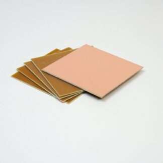
The Marvel of Copper Clad
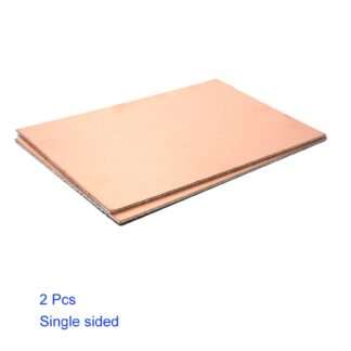
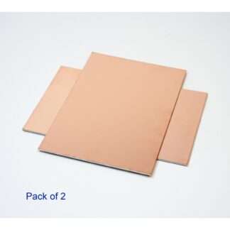
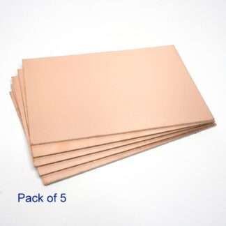
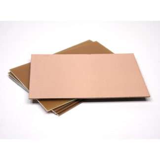
Copper clad, also known as copper-clad laminate, is a material that combines a thin layer of copper with a non-conductive substrate. This unique composition grants it the best of both worlds – the conductivity of copper and the flexibility of a substrate. This makes it an ideal choice for a wide range of applications.
One of the key benefits of copper clad is its versatility. It can be easily cut and shaped to fit the specific requirements of your project, making it an excellent option for prototypes and custom designs. Additionally, the copper layer provides excellent electrical conductivity, ensuring efficient signal transmission and reducing power losses.
The Power of PCBs
PCBs, or Printed Circuit Boards, are the backbone of almost every electronic device we use today. These flat boards consist of multiple layers of copper tracks and pads that connect different electronic components. The traces and pads are etched onto the surface of the board, allowing for precise and reliable connections.
The use of PCBs offers numerous advantages. Firstly, they save space by eliminating the need for bulky point-to-point wiring. This compact design makes PCBs perfect for small electronic devices, where every square inch matters. Secondly, the use of copper tracks ensures efficient signal flow, minimizing the risk of interference and signal degradation. Lastly, PCBs are highly reliable and can withstand extreme temperatures, making them suitable for a wide range of environments.
The Perfect Combination
When copper clad and PCBs come together, magic happens. These two components complement each other perfectly, resulting in high-performance electronics. Copper clad provides a sturdy and conductive base, while PCBs allow for easy and organized circuitry.
By using copper clad as the foundation, PCBs can be easily mounted and soldered onto the substrate, ensuring a secure and reliable connection. The combination of copper clad and PCBs also enhances signal integrity, reducing the risk of electromagnetic interference and ensuring smooth operation.
Whether you’re a hobbyist, a professional, or an electronics enthusiast, the beauty of copper clad and PCBs is undeniable. The possibilities these components offer are endless, allowing you to bring your innovative ideas to life.